Technical Note
15/18
www.rohm.com
2009.08 - Rev.A
?2009 ROHM Co., Ltd. All rights reserved.
BD9153MUV
?SPAN class="pst BD9153MUV-E2_2471427_7">BD9153MUV Cautions on PC Board layout
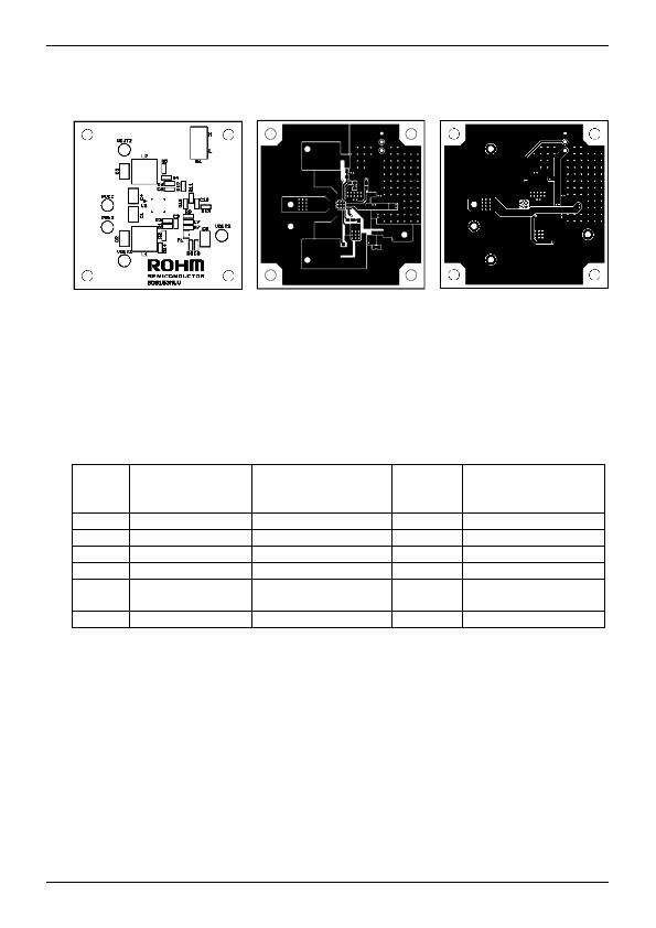
Fig.42 Layout diagram
` Lay out the input ceramic capacitor CIN closer to the pins PVCC and PGND, and the output capacitor Co closer to
the pin PGND.
a Lay out CITH and RITH between the pins ITH and GND as neat as possible with least necessary wiring.
; VQFN024V4040 (BD9153MUV) has thermal PAD on the reverse of the package.
The package thermal performance may be enhanced by bonding the PAD to GND plane which take a large area of PCB.
?SPAN class="pst BD9153MUV-E2_2471427_7">Recommended components Lists on above application
Symbol
Part
Value
Manufacturer
Series
L1,2 Coil
2.2礖
TDK LTF5022-2R2N3R2
CIN1,CIN2 Ceramic capacitor
22礔
Murata GRM32EB11A226KE20
Cout1,Cout2 Ceramic capacitor
22礔
Murata GRM31CB30J226KE18
CITH1 Ceramic capacitor
VOUT1=3.3V 680pF Murata GRM18 Series
RITH1 Resistance
VOUT1=3.3V 39k&
Rohm MCR03 Series
CITH2 Ceramic capacitor
VOUT2=1.2V 680pF Murata GRM18 Series
RITH2 Resistance
VOUT2=1.2V 12k&
Rohm MCR03 Series
Cfb Ceramic capacitor
56pF
Murata GRM18 Series
M1 Nch MOS FET
-
Rohm RTF015N03
;The parts list presented above is an example of recommended parts. Although the parts are sound, actual circuit
characteristics should be checked on your application carefully before use. Be sure to allow sufficient margins to
accommodate variations between external devices and BU9153MUV when employing the depicted circuit with other
circuit constants modified. Both static and transient characteristics should be considered in establishing these margins.
When switching noise is substantial and may impact the system, a low pass filter should be inserted between the VCC and
PVCC pins, and a schottky barrier diode or snubber established between the SW and PGND pins.
Silk screen
Top Layer
Bottom Layer
发布紧急采购,3分钟左右您将得到回复。
相关PDF资料
CAT2300VP2-GT3
IC SENSE FET CONTROLLER 8TDFN
CAT34TS02VP2GT4A
IC TEMP SENSOR 2K MEMORY 8TDFN
CAT6095VP2-GT4
IC TEMP SENSOR STAND ALONE 8TDFN
DS1621S+
IC THERMOMETER/STAT DIG 8-SOIC
DS1624S+T&R
IC THERM/EEPROM DIG 256BYT 8SOIC
DS1626S+
IC THERMOMETER/STAT DIG 8-SOIC
DS1629S+T&R
IC THERM/RTC/CALENDAR DIG 8-SOIC
DS1631S+T&R
IC THERMOMETER DIG HI-PREC 8SOIC
相关代理商/技术参数
BD9160FVM
制造商:ROHM 制造商全称:Rohm 功能描述:1ch DC/DC Converter Controller IC with Built-in Synchronous Rectifier
BD9160FVM-TR
制造商:ROHM Semiconductor 功能描述:Cut Tape
BD9161FVM
制造商:ROHM 制造商全称:Rohm 功能描述:Output 1.5A or Less High-efficiency Step-down Switching Regulator with Built-in Power MOSFET
BD9161FVM_12
制造商:ROHM 制造商全称:Rohm 功能描述:2.5V to 4.5V, 0.6A 1ch Synchronous Buck Converter Integrated FET
BD9161FVM-LBTR
功能描述:Buck Switching Regulator IC Positive Adjustable 1V 1 Output 600mA 8-VSSOP, 8-MSOP (0.110", 2.80mm Width) 制造商:rohm semiconductor 系列:- 包装:剪切带(CT) 零件状态:有效 功能:降压 输出配置:正 拓扑:降压 输出类型:可调式 输出数:1 电压 - 输入(最小值):2.5V 电压 - 输入(最大值):4.5V 电压 - 输出(最小值/固定):1V 电压 - 输出(最大值):3.3V 电流 - 输出:600mA 频率 - 开关:1MHz 同步整流器:是 工作温度:-25°C ~ 85°C(TA) 安装类型:表面贴装 封装/外壳:8-VSSOP,8-MSOP(0.110",2.80mm 宽) 供应商器件封装:8-MSOP 标准包装:1
BD9161FVM-TR
功能描述:开关变换器、稳压器与控制器 High Eff. Stepdown Sw Reg 0.6A 2.5-4.5V RoHS:否 制造商:Texas Instruments 输出电压:1.2 V to 10 V 输出电流:300 mA 输出功率: 输入电压:3 V to 17 V 开关频率:1 MHz 工作温度范围: 安装风格:SMD/SMT 封装 / 箱体:WSON-8 封装:Reel
BD-9178G
制造商:Distributed By MCM 功能描述:2.4Ghz Wireless USB Mouse
BD920
功能描述:ANTENNA GSM / UMTS PANEL 12DB - 制造商:b&b smartworx, inc. 系列:- 零件状态:在售 配件类型:天线 配套使用产品/相关产品:- 标准包装:1